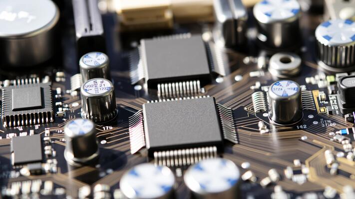
The semiconductor industry is rapidly evolving, demanding higher precision, cleaner processing environments, and more robust materials than ever before. As chip architectures become increasingly compact and intricate, traditional materials often fall short of performance requirements. In this context, high-density tungsten sheets have emerged as essential components in semiconductor manufacturing, offering unmatched density, thermal stability, and radiation shielding properties. But what exactly makes tungsten sheet indispensable for semiconductors, and how is it used in these critical applications?
At Heeger Metal, we specialize in high-density tungsten sheets, ensuring optimal performance for industrial and scientific applications.
Why Is High-Density Tungsten Important in Semiconductor Manufacturing?
Semiconductor fabrication involves processes such as ion implantation, photolithography, and plasma etching, which expose materials to extreme conditions, including high temperatures, high-energy particles, and chemical interactions. Materials used in these processes must remain dimensionally stable and chemically inert. Tungsten, with its exceptionally high melting point (3422°C), excellent wear resistance, and chemical compatibility, is one of the few metals that meet these stringent requirements.
| Property | Tungsten Sheet |
| Density (g/cm³) | 19.25 |
| Melting Point (°C) | 3422 |
| Thermal Conductivity (W/m·K) | 174 |
| Electrical Resistivity (μΩ·cm) | 5.5 |
| Coefficient of Thermal Expansion (µm/m·K) | 4.5 |
| Hardness (Vickers, HV) | ~343 |
| Plasma Resistance | Excellent |
| Outgassing in Vacuum | Minimal |
| Radiation Shielding Capability | High |
| Chemical Stability | Excellent |
| Surface Oxidation Resistance | Moderate (improves with coatings) |
| Machinability | Difficult (requires precision tools) |
Tungsten’s combination of high density and low outgassing makes it suitable for vacuum environments in tools like chemical vapor deposition (CVD) chambers and ion implanters. Its inertness helps maintain purity in cleanroom operations.
What Are the Key Applications of Tungsten Sheets in the Semiconductor Industry?
- Ion Implantation Systems: Tungsten sheets are used as collimators, apertures, and beam stoppers to control and absorb high-energy ions. The density of tungsten helps reduce radiation scatter and prevent damage to surrounding components.
- Sputtering Targets and Masks: In physical vapor deposition (PVD) processes, tungsten sheets serve as masks or shields to focus plasma streams and control material deposition.
- Wafer Handling Components: Tungsten is used for chucks, carriers, and platforms where high thermal stability and dimensional integrity are crucial.
- Radiation Shielding: Equipment that operates near X-ray sources or plasma frequently integrates tungsten shielding to protect sensitive parts and ensure operator safety.
Explore our high-density tungsten sheets.
How Does Tungsten Outperform Other Shielding Materials in Semiconductor Tools?
Unlike materials such as stainless steel or aluminum, tungsten provides far greater density and radiation attenuation. This is especially important in next-generation extreme ultraviolet (EUV) lithography and ion beam processing, where particle control and radiation management are critical.
| Shielding Material | Relative Gamma Shielding (1 mm thick) | Thermal Resistance | Chemical Stability |
| Tungsten | 1.0 (baseline) | Excellent | Excellent |
| Lead | 0.8 | Poor | Poor |
| Steel | 0.4 | Fair | Good |
| Aluminum | 0.2 | Good | Moderate |
Tungsten enables thinner, more compact shielding without sacrificing protection. Its high thermal mass also makes it effective in heat dissipation, preventing hotspots in dense equipment setups.
What Manufacturing Options Are Available for Tungsten Sheets?
Tungsten sheets can be produced using powder metallurgy, followed by hot rolling or sintering. They can be machined, polished, or surface-treated depending on the application. Common options include:
- Thickness Range: 0.1 mm to 50 mm
- Width: Up to 500 mm
- Surface Finish: Ground, polished, or rough-machined
- Purity: >99.95% standard; higher available on request
Tungsten sheets for semiconductor applications are typically manufactured to ultra-high vacuum (UHV) standards, ensuring minimal impurities and low outgassing.
Request a custom quote for High-Density Tungsten Sheets.
What Quality Standards Do Tungsten Sheets Meet?
Tungsten sheets used in high-tech sectors such as semiconductors and vacuum electronics must comply with stringent international quality standards to ensure consistent performance, reliability, and compatibility in ultra-clean environments. These standards govern everything from material purity and mechanical strength to vacuum compatibility and thermal behavior.
Below is a summary of key quality standards commonly associated with tungsten sheet manufacturing:
| Standard | Description |
| Specifies requirements for flat-rolled tungsten, including chemical composition, thickness, flatness, and mechanical properties. | Specifies requirements for flat-rolled tungsten including chemical composition, thickness, flatness, and mechanical properties. |
| ISO 9001 | Ensures the manufacturer has a quality management system in place for consistent production and traceability. |
| RoHS Compliant | Confirms the product is free from hazardous substances as per EU directives. |
These standards help guarantee the tungsten sheet meets the exacting needs of applications in the semiconductor and microelectronics industries, where cleanliness, consistency, and thermal stability are paramount.
What Are the Benefits of Using Tungsten Sheets in Semiconductor Fabrication?
- High Process Stability: Ensures consistent performance in plasma and ion environments
- Extended Component Lifespan: Resists wear, erosion, and heat damage
- Superior Cleanroom Compatibility: Low contamination risk due to low vapor pressure
- Compact Equipment Design: High density allows for smaller, more efficient shielding structures
Why Tungsten Sheets Are the Future of Semiconductor Engineering
As semiconductor tools become more complex and performance expectations rise, materials that offer thermal, mechanical, and chemical superiority are crucial. High-density tungsten sheets meet these needs across a variety of toolsets and process stages. Their unique properties support higher device yields, better process control, and longer equipment lifespans.
Heeger Metal provides premium-grade tungsten sheets engineered for semiconductor applications. We offer tight dimensional tolerances, high purity, and custom configurations to meet the specific requirements of leading-edge fabs and toolmakers worldwide.
Looking for high-density tungsten sheets? Contact us today!