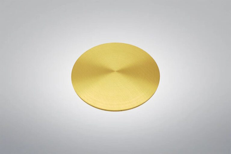
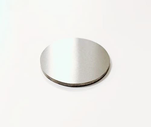
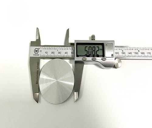
Palladium Sputtering Target
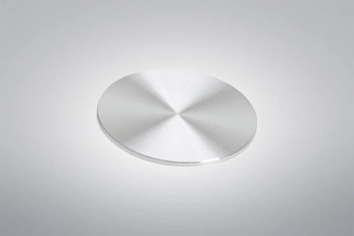
Palladium Sputtering Target
Purity: ≥99.95%, or customized
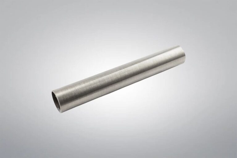
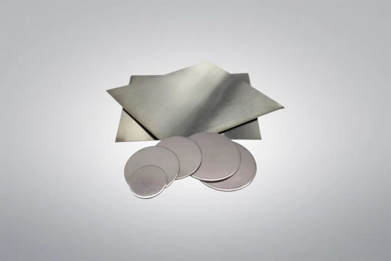
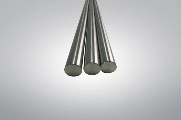
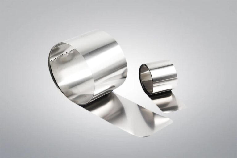
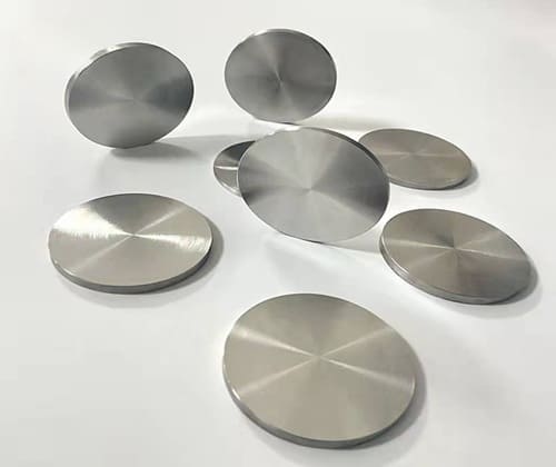
Shape: Disc, Rectangular, Tube, or customized
Palladium Sputtering Target is made from high-purity palladium metal, widely applied in thin film deposition technologies. As a leading supplier and manufacturer of premium palladium products, Heeger Metal leverages advanced technology to deliver high-quality palladium sputtering targets for various applications.
Or email us at sales@heegermaterials.com.Palladium Sputtering Target Data Sheet
| Reference Code: | HTST17 |
| CAS: | 7440-05-3 |
| Purity: | ≥99.95%, or customized |
| Density: | 12.023 g/cm3 |
| Melting Point: | 1554℃ |
| Boiling Point: | 2970℃ |
| Shape: | Disc, Rectangular, Tube, or customized |
| Bonding: | Bongding or Unbonding |
Palladium Sputtering Target Description
Palladium (Pd) has the unique ability to absorb and release hydrogen, making it an ideal choice for hydrogenation and purification systems. Palladium Sputtering Target is made of high-purity palladium metal. It is widely used in film deposition technologies, particularly in fields such as semiconductors, optical coatings, flat-panel displays, and solar cells. In the magnetron sputtering process, the palladium sputtering target is used to deposit a uniform thin film onto the substrate. Heeger Metal can supply high-precision palladium sputtering targets in various specifications to suit industrial and research applications, ensuring optimal performance and cost-effectiveness.
Palladium Sputtering Target Specifications
| Material Type | Palladium |
| Symbol | Pd |
| Atomic Weight | 106.42 |
| Atomic Number | 46 |
| Color/Appearance | Silvery White Metallic |
| Thermal Conductivity | 72 W/m.K |
| Melting Point (°C) | 1,554 |
| Coefficient of Thermal Expansion | 11.8 x 10⁻⁶/K |
| Theoretical Density (g/cc) | 12.02 |
| Z Ratio | 0.357 |
| Sputter | DC |
| Max Power Density (Watts/Square Inch) | 100* |
| Type of Bond | Indium, Elastomer |
| Comments | Alloys with refractory metals. |
Palladium Sputtering Target Stock Dimensions
| Circular Sputtering Targets | Diameter | 1.0″ 2.0″ 3.0″ 4.0″ 5.0″ 6.0″ up to 21″ |
| Rectangular Sputtering Targets | Width x Length | 5″ x 12″ 5””x 15″ 5″ x 20″ 5″ x 22″ 6″ x 20″ |
| Thickness | 0.125″, 0.25″ | |
Palladium Sputtering Target Manufacturing Processes
- Material Preparation: Select high-purity palladium raw material (typically ≥99.95% purity)
- Vacuum Induction Melting: A high-precision melting process using vacuum induction to ensure uniform alloy composition and eliminate contaminants.
- Annealing: A heat treatment process to relieve internal stresses, improve material properties, and achieve desired hardness and ductility.
- Rolling: The material is passed through rollers to reduce thickness, increase length, and refine the structure for further processing.
- Stamping: Using mechanical presses to shape or cut the material into specific forms, ensuring precise dimensions and consistency.
- Metallographic Testing: Detailed analysis of the material’s microstructure to ensure the quality and integrity of the alloy before further processing.
- Machining: Precision machining processes (such as turning, milling, or grinding) to achieve the desired shapes and tolerances.
- Dimensional inspection: Measuring and verifying the dimensions of the product to ensure they meet the required specifications.
- Cleaning: Thorough cleaning of the material to remove any residue, oils, or contaminants left from the manufacturing processes.
- Final Inspection: A comprehensive inspection process to ensure the product meets all quality and functional standards.
Palladium Sputtering Target Applications
- Electronics Industry: Palladium sputtering targets are widely used in thin film deposition, particularly in semiconductor manufacturing, for creating electrode layers in integrated circuits, capacitors, and sensors.
- Optical Coatings: Palladium sputtering targets are used to produce high-reflection optical thin films, which are commonly applied in laser systems, optical lenses, and displays.
- Solar Cells: Palladium sputtering targets are used as electrode materials in solar cells, helping to improve their efficiency.
- Flat-Panel Displays: Palladium sputtering targets are used in the production of conductive thin films in flat-panel displays, ensuring the performance and stability of the displays.
- Magnetic Materials: Palladium sputtering targets are used in the deposition of thin films for magnetic materials, which are applied in hard disk drives and magnetic recording devices.
- Chemical Industry: Palladium sputtering targets are used as catalysts in organic synthesis reactions, particularly in hydrogenation and dehydrogenation processes.
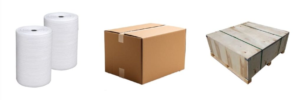
Palladium Sputtering Target Packaging
Palladium Sputtering Target is carefully placed in wooden cases or cartons with additional soft materials to support and prevent shifting during transportation. This packaging method guarantees the integrity of the products throughout the delivery process.
Palladium Properties
Download
Get A Quote
We will check and get back to you in 24 hours.
Sputtering Targets Products
Heeger Metal offers a wide selection of high-performance sputtering targets made from materials like titanium, copper, aluminum, and rare earth metals. Our custom sputtering targets are precision-engineered to meet the demands of industries such as semiconductor manufacturing, photovoltaics, and electronics. With superior purity and consistency, our sputtering targets deliver exceptional film deposition performance, making them ideal for thin-film coating, sputtering, and PVD (Physical Vapor Deposition) applications.