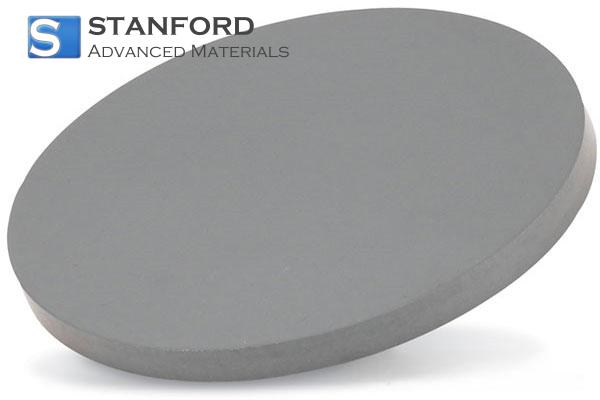
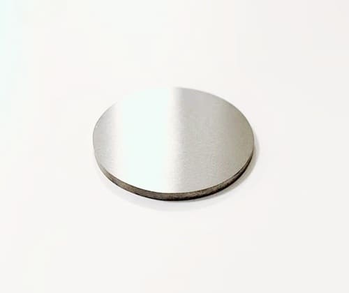
Palladium Sputtering Target
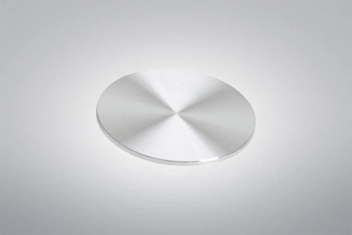
Palladium Sputtering Target
Reinheit: ≥99.95%, oder kundenspezifisch
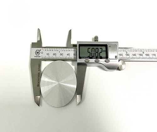
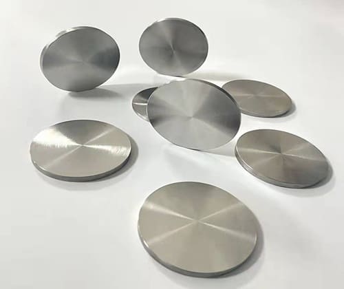
Form: Scheibe, Rechteckig, Rohr, oder kundenspezifisch
Palladium-Sputtertargets werden aus hochreinem Palladiummetall hergestellt und finden breite Anwendung in der Dünnschichttechnik. Als führender Anbieter und Hersteller von Premium-Palladiumprodukten nutzt Heeger Metal fortschrittliche Technologien, um hochwertige Palladium-Sputtertargets für verschiedene Anwendungen zu liefern.
Oder senden Sie uns eine E-Mail an sales@heegermaterials.com.
Datenblatt Palladium Sputtering Target
| Referenz-Code: | HTST17 |
|---|---|
| CAS: | 7440-05-3 |
| Reinheit: | ≥99.95%, oder kundenspezifisch |
| Die Dichte: | 12,023 g/cm3 |
| Schmelzpunkt: | 1554℃ |
| Siedepunkt: | 2970℃ |
| Die Form: | Scheibe, Rechteckig, Rohr, oder kundenspezifisch |
| Bindung: | Bindung oder Entbindung |
Palladium Sputtering Target Beschreibung
Palladium (Pd) hat die einzigartige Fähigkeit, Wasserstoff zu absorbieren und freizusetzen, was es zu einer idealen Wahl für Hydrier- und Reinigungssysteme macht. Palladium-Sputtering-Targets werden aus hochreinem Palladiummetall hergestellt. Es findet breite Anwendung in der Beschichtungstechnologie, insbesondere in Bereichen wie Halbleiter, optische Beschichtungen, Flachbildschirme und Solarzellen. Beim Magnetron-Sputterverfahren wird das Palladium-Sputtertarget verwendet, um eine gleichmäßige dünne Schicht auf das Substrat aufzubringen. Heeger Metal kann hochpräzise Palladium-Sputtertargets in verschiedenen Spezifikationen für Industrie- und Forschungsanwendungen liefern, die optimale Leistung und Kosteneffizienz gewährleisten.
Spezifikationen für Palladium-Sputtering-Targets
| Material Typ | Palladium |
|---|---|
| Symbol | Pd |
| Atomares Gewicht | 106.42 |
| Ordnungszahl | 46 |
| Farbe/Erscheinungsbild | Silberweiß Metallic |
| Wärmeleitfähigkeit | 72 W/m.K |
| Schmelzpunkt (°C) | 1,554 |
| Wärmeausdehnungskoeffizient | 11,8 x 10⁻⁶/K |
| Theoretische Dichte (g/cc) | 12.02 |
| Z-Verhältnis | 0.357 |
| Sputter | DC |
| Maximale Leistungsdichte (Watt/Quadratzoll) | 100* |
| Art der Anleihe | Indium, Elastomer |
| Kommentare | Legierungen mit hochschmelzenden Metallen. |
Palladium Sputtering Target Lager Abmessungen
| Zirkulare Sputtering-Targets | Durchmesser | 1.0″ 2.0″ 3.0″ 4.0″ 5.0″ 6.0″ bis zu 21″. |
|---|---|---|
| Rechteckige Sputtering-Targets | Breite x Länge | 5″ x 12″ 5””x 15″ 5″ x 20″ 5″ x 22″ 6″ x 20″ |
| Dicke | 0.125″, 0.25″ | |
Herstellungsverfahren für Palladiumsputtertargets
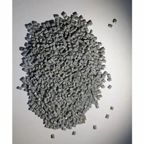
- Vorbereitung des Materials: Auswahl von hochreinem Palladium-Rohmaterial (typischerweise ≥99,95%-Reinheit)
- Vakuum-Induktionsschmelzen: Ein hochpräzises Schmelzverfahren mit Vakuuminduktion, das eine gleichmäßige Legierungszusammensetzung gewährleistet und Verunreinigungen eliminiert.
- Glühen: Ein Wärmebehandlungsverfahren zum Abbau innerer Spannungen, zur Verbesserung der Materialeigenschaften und zum Erreichen der gewünschten Härte und Duktilität.
- Rollender: Das Material wird durch Walzen geführt, um die Dicke zu verringern, die Länge zu vergrößern und die Struktur für die weitere Verarbeitung zu verfeinern.
- Stanzen: Mit Hilfe mechanischer Pressen wird das Material in bestimmte Formen gebracht oder geschnitten, um genaue Abmessungen und Konsistenz zu gewährleisten.
- Metallographische Prüfung: Detaillierte Analyse der Mikrostruktur des Materials, um die Qualität und Unversehrtheit der Legierung vor der Weiterverarbeitung sicherzustellen.
- Bearbeitung: Präzisionsbearbeitungsverfahren (wie Drehen, Fräsen oder Schleifen), um die gewünschten Formen und Toleranzen zu erreichen.
- Prüfung der Dimensionen: Messen und Prüfen der Abmessungen des Produkts, um sicherzustellen, dass sie den geforderten Spezifikationen entsprechen.
- Reinigung: Gründliche Reinigung des Materials, um alle Rückstände, Öle oder Verunreinigungen aus dem Herstellungsprozess zu entfernen.
- Abschließende Inspektion: Ein umfassendes Prüfverfahren, um sicherzustellen, dass das Produkt alle Qualitäts- und Funktionsstandards erfüllt.
Palladium Sputtering Target Anwendungen
- Elektronikindustrie: Palladium-Sputtertargets werden in der Dünnschichtabscheidung, insbesondere in der Halbleiterherstellung, zur Herstellung von Elektrodenschichten in integrierten Schaltkreisen, Kondensatoren und Sensoren eingesetzt.
- Optische Beschichtungen: Palladium-Sputter-Targets werden zur Herstellung hochreflektierender optischer Dünnschichten verwendet, die häufig in Lasersystemen, optischen Linsen und Displays eingesetzt werden.
- Solarzellen: Palladium-Sputter-Targets werden als Elektrodenmaterial in Solarzellen verwendet und tragen zur Verbesserung ihrer Effizienz bei.
- Flachbildschirme: Palladium-Sputter-Targets werden bei der Herstellung von leitfähigen Dünnschichten für Flachbildschirme verwendet, um die Leistung und Stabilität der Displays zu gewährleisten.
- Magnetische Materialien: Palladium-Sputtertargets werden bei der Abscheidung dünner Schichten für magnetische Materialien verwendet, die in Festplattenlaufwerken und magnetischen Aufzeichnungsgeräten zum Einsatz kommen.
- Chemische Industrie: Palladium-Sputter-Targets werden als Katalysatoren in organischen Synthesereaktionen eingesetzt, insbesondere in Hydrierungs- und Dehydrierungsprozessen.
Palladium Sputtering Target Verpackung
Palladium Sputtering Target wird sorgfältig in Holzkisten oder Kartons mit zusätzlichen weichen Materialien verpackt, um ein Verrutschen während des Transports zu verhindern. Diese Verpackungsmethode garantiert die Unversehrtheit der Produkte während des gesamten Liefervorgangs.
Palladium-Eigenschaften
Herunterladen
Angebot einholen
Wir werden das prüfen und uns innerhalb von 24 Stunden bei Ihnen melden.
Sputtering Targets Produkte
Heeger Metal bietet eine große Auswahl an Hochleistungs-Sputtertargets aus Materialien wie Titan, Kupfer, Aluminium und Seltenerdmetallen. Unsere kundenspezifischen Sputtertargets sind präzisionsgefertigt, um den Anforderungen von Branchen wie der Halbleiterherstellung, Photovoltaik und Elektronik gerecht zu werden. Dank ihrer überragenden Reinheit und Konsistenz bieten unsere Sputtertargets eine außergewöhnliche Leistung bei der Schichtabscheidung und sind damit ideal für die Dünnfilmbeschichtung, das Sputtern und PVD-Anwendungen (Physical Vapor Deposition).